Core Takeaway: Moore’s Law as we knew it—shrinking transistors every two years—has hit physical and economic limits. The semiconductor industry is now reinventing progress through chiplets, 3D stacking, domain-specific architectures, and co-design across hardware, software, and materials. Performance is no longer measured by transistor count alone but by metrics like performance per watt and effective compute density. This shift marks a more creative, system-level era where innovation comes from integration, not just miniaturization.
Why Traditional Scaling Hit a Wall
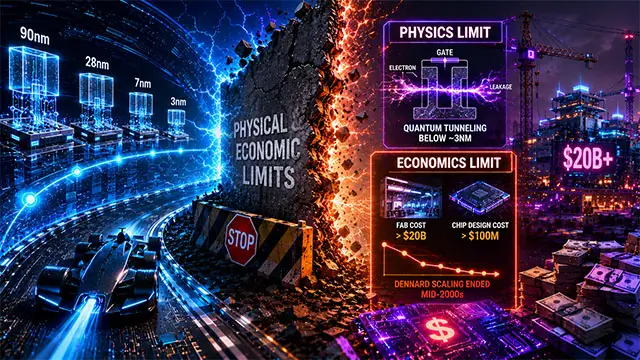
For decades, chip progress meant smaller transistors and higher clock speeds. But that straightforward path is now blocked by two barriers:
• Physics: Below roughly 3 nanometers, quantum tunneling causes electrons to leak through transistor gates, degrading reliability and power efficiency.
• Economics: A state-of-the-art fabrication plant costs over $20 billion, and designing a single leading-edge chip can run hundreds of millions of dollars. Dennard scaling—the once-reliable expectation that smaller transistors automatically lower power density—ended in the mid-2000s.
In short, the old formula of “shrink the transistor, boost the clock” no longer delivers cost-effective improvements.
The Rise of Heterogeneous Integration and Chiplets
Instead of a single monolithic die that tries to do everything, chip architects now assemble systems from multiple specialized dies—an approach called heterogeneous integration. At the center of this revolution are chiplets: small, modular integrated circuits stitched together on a single package with high-speed interconnects.
• A modern processor might combine separate chiplets for CPU, graphics, AI acceleration, and input/output, each manufactured on its optimal process node.
• Defects are contained to one chiplet instead of scrapping an entire large die, dramatically improving manufacturing yield and lowering costs.
• Examples: AMD’s EPYC and Ryzen processors, Intel’s Meteor Lake, and Apple’s M series Ultra chips.
The open standard Universal Chiplet Interconnect Express (UCIe), backed by over 120 companies, aims to create a plug and play ecosystem where chiplets from different vendors mix seamlessly—much like USB standardized peripherals.
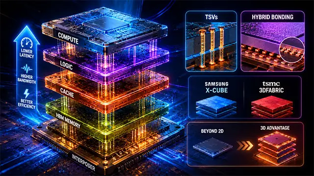
Stacking Upward: 3D Packaging
If transistors cannot be packed more densely in two dimensions, the next frontier is the third. Advanced 3D packaging stacks multiple layers of silicon vertically, connected by microscopic through silicon vias (TSVs).
• Stacking shortens data travel distance, reducing latency and energy consumption while increasing bandwidth.
• The most advanced technique, hybrid bonding, fuses copper pads between stacked dies without solder bumps, achieving sub micron pitch connections.
• Samsung’s “X Cube” and TSMC’s “3D Fabric” portfolio are moving this technology into high volume production.
The result: processors where compute and memory are fused into a single three dimensional block, delivering performance levels traditional planar scaling could never reach.
Domain Specific Architectures: Hardware Purpose Built for the Job
General purpose processors are giving way to chips that incorporate dedicated hardware accelerators tailored to specific tasks.
• Google’s TPUs and Apple’s Neural Engine accelerate machine learning.
• NVIDIA’s Grace Hopper Superchip pairs a CPU, GPU, and high bandwidth memory, optimized for training large language models.
The era of one size fits all silicon is fading. Heterogeneous collections of task specific engines, integrated on a single package, now deliver the best results.
The Co Design Revolution: Hardware, Software, and Materials
Progress increasingly depends on simultaneous innovation across disciplines.
• New materials: Ruthenium is replacing copper in critical interconnect layers for lower resistance at tiny scales. Gallium nitride (GaN) and silicon carbide (SiC) are replacing silicon in power electronics for greater efficiency.
• Software and compilers are being redesigned to distribute code optimally across clusters of heterogeneous chiplets.
• AI itself now helps design chips—tools like Synopsys’ DSO.ai use reinforcement learning to explore design spaces and optimize floor plans, potentially cutting weeks from the design cycle.
This tight coupling of hardware, software, and materials is the new engine of chip innovation.
New Metrics for a New Era
The definition of progress has shifted:
• Performance per watt
• Effective compute density
• Memory bandwidth per joule
• Total cost of ownership
A chip with fewer transistors can deliver better real-world performance through smarter architecture and packaging. The industry increasingly measures success by how effectively it solves real problems—rendering a video game, training a large language model, or analyzing medical images at the edge—not by transistor count alone.
Conclusion
The simple transistor sprint that defined Moore’s Law for over 50 years has given way to a richer, multi-dimensional approach. The next Moore’s Law is written in chiplets, 3D stacking, domain specific accelerators, and deep co design.